Key Software / Application
1. Fusion 360 / Solidworks
Design mechanical prototypes (rigid body, bearing, linkage system, dowel pins, etc.)
2. Arduino
Finite state machine programming and integrating mechanical/electrical components together
3. CircuitLab
Circuit schematic maker and simulator
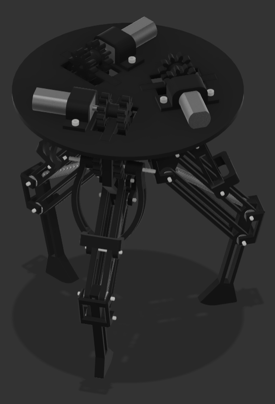
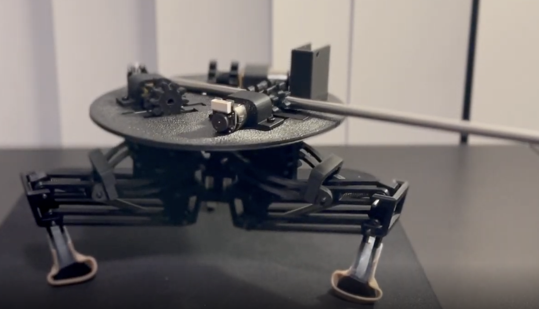
Figure 1. Full Assembly Isometric View
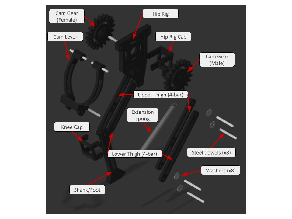
Figure 2. Full Leg Exploded View
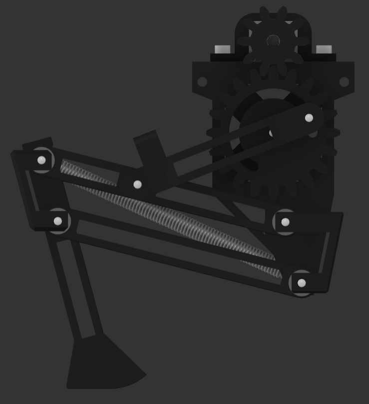
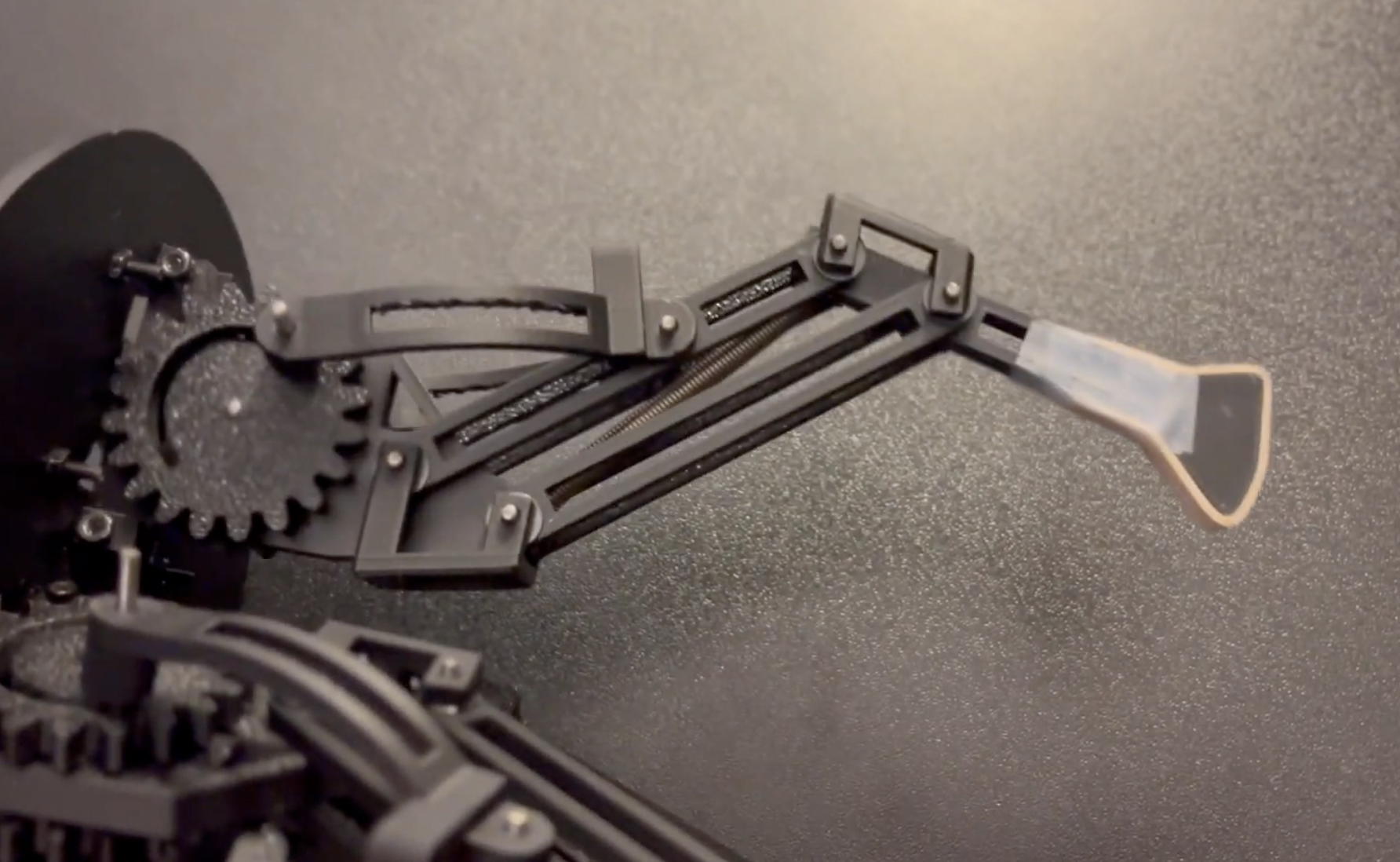
Figure 3. Leg Flexion
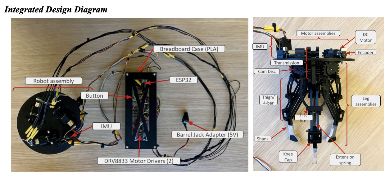
Figure 4. Labeled Diagram of Assembly (including Electronics)
4-Bar Linkage Calculations
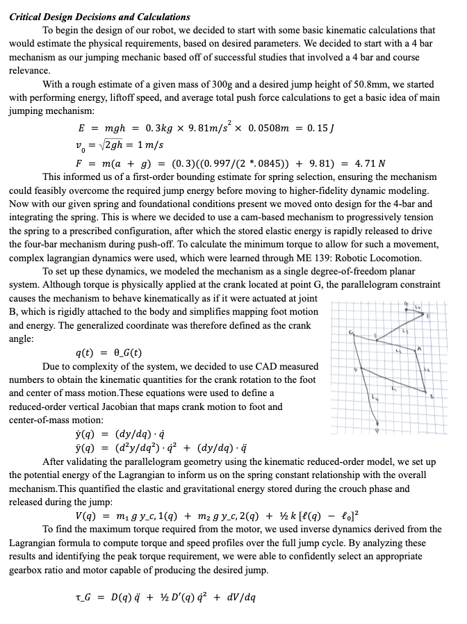
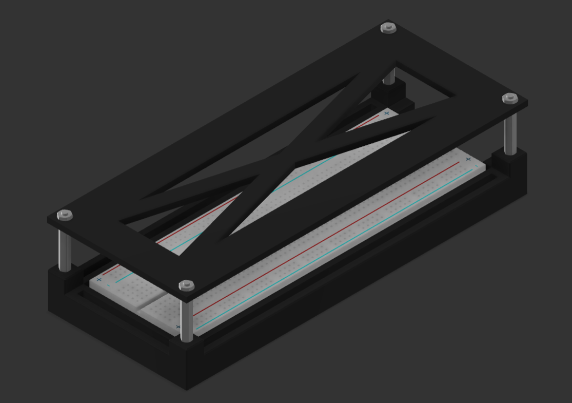
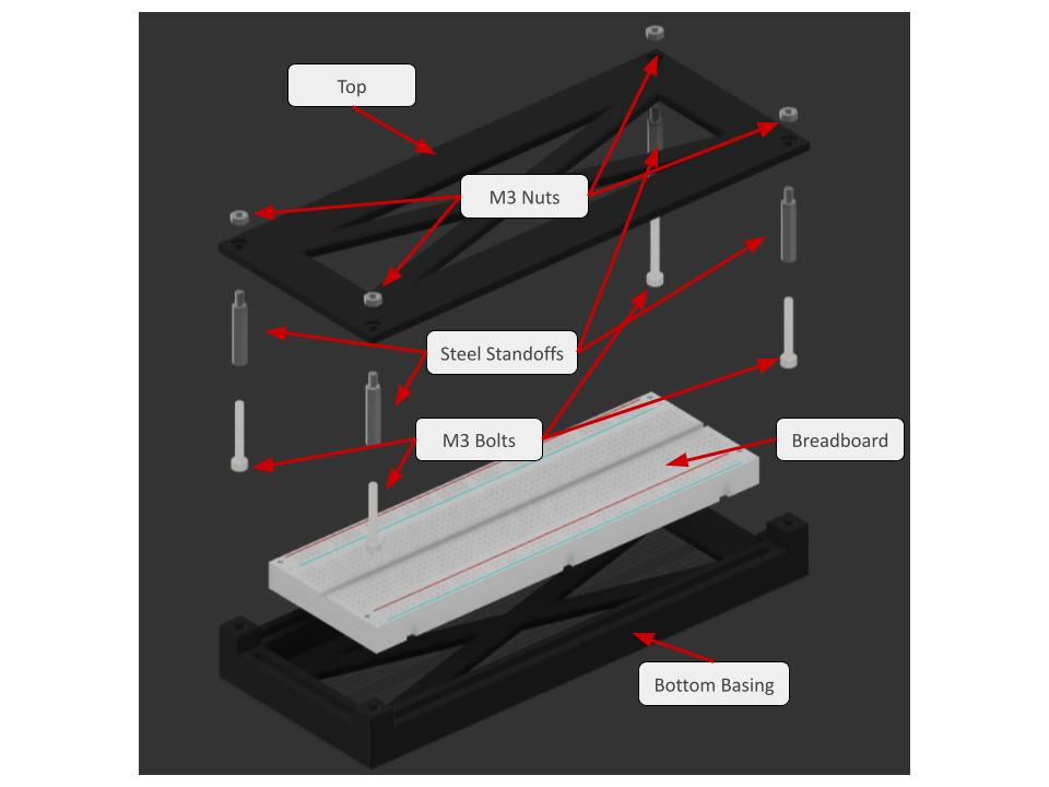
Figure 5 and 6. Full Assembly of Breadboard Casing + Detailed/Exploded View
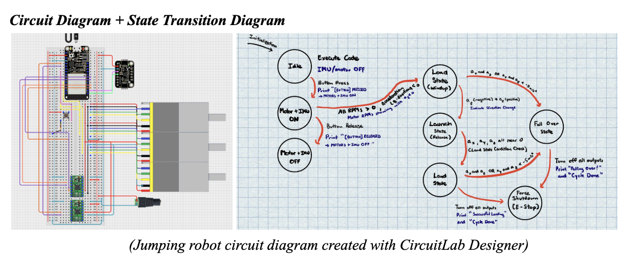
The circuit connects a microcontroller to motors, motor drivers, an IMU sensor, and a button to control motion and sensing. The state transition diagram shows how the robot moves through stages like idle, windup, launch, flight, landing, and shutdown based on button input and IMU acceleration data. Together, they explain how the robot safely powers on, jumps, detects its motion, and turns off after completing a cycle or if it falls over.
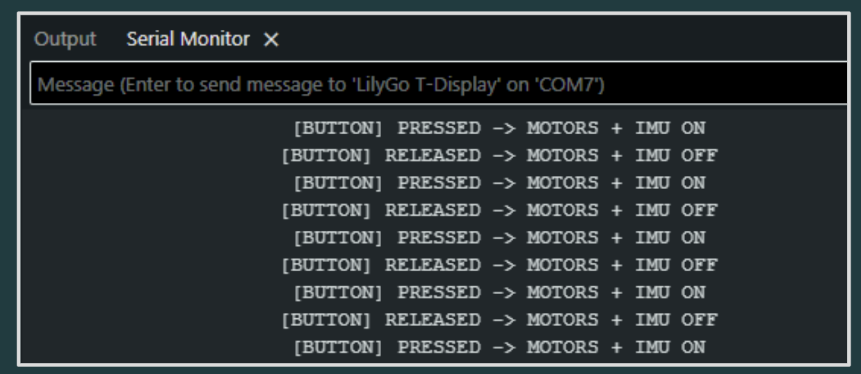
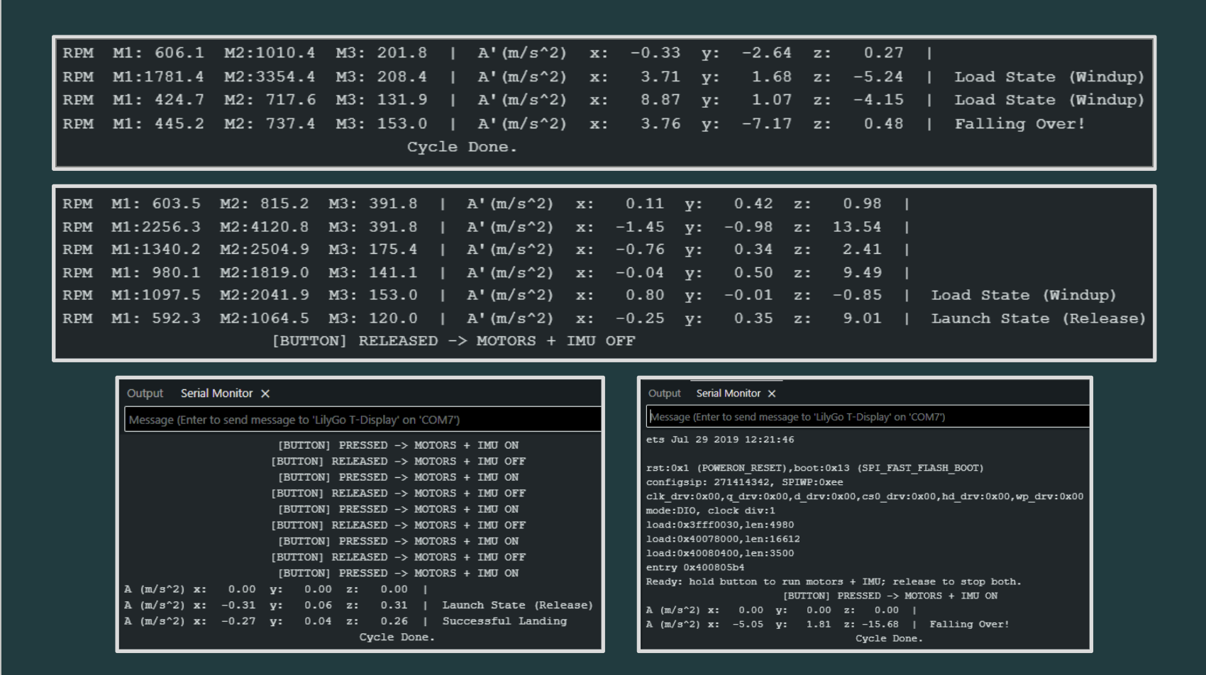
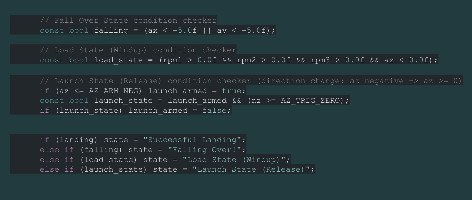
Figure 7. Snapshots of Relevant Output on Serial Monitor (IMU, Motor RPM, and resulting states)
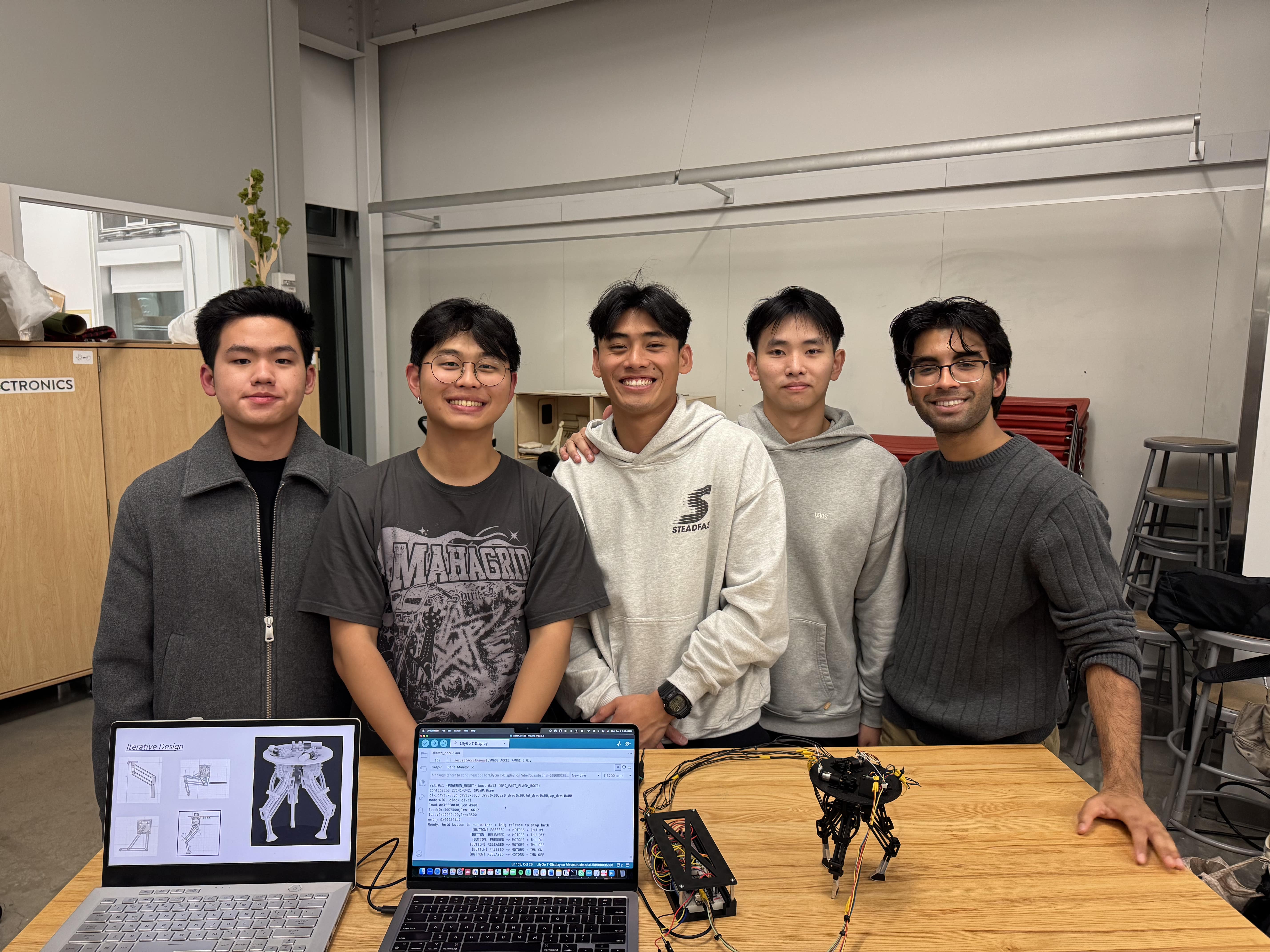
Through the ME102B Project, I learned how mechanical design, electronics, and software must work together for a system to function reliably. I improved my skills in component integration by wiring motors, sensors, and drivers correctly and ensuring they communicated properly with the microcontroller. I also strengthened my software programming skills by implementing a state machine that used sensor data to control timing, motion, and safety behaviors during the jump cycle. Our team also won the Best Mechanical Design Award!
Video 1. Jump Mechanics (Click on Image!)
Video 2. Leg Full Extension Mechanism